Sharing a Classic Overvoltage Protection Circuit Design

Here are the three scenarios:
Input voltage is less than 5.1V:
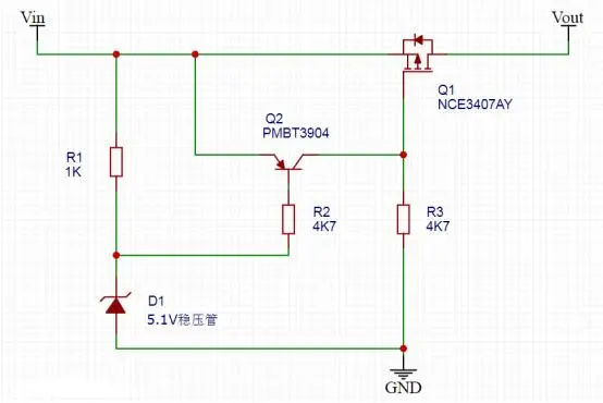
When the input voltage is 5V, the voltage across the zener diode D1 is 5.1V. Since the input voltage is less than 5.1V, D1 is not yet in its zener breakdown region, so it does not conduct. The transistor also does not conduct (since its base and emitter voltages are both 5V, resulting in Vbe = 0).

Input voltage is between 5.1V and 5.7V:
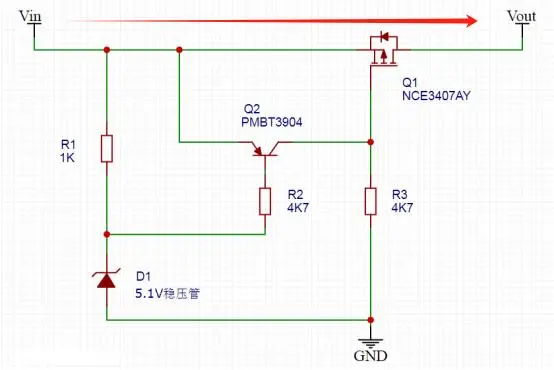
When the input voltage is 5.4V, greater than the zener voltage of D1 (5.1V), D1 conducts and stabilizes at 5.1V. The voltage across the transistor's base-emitter junction is Vbe = 5.1V - 5.4V = -0.3V, which is below the threshold voltage required for conduction (-0.6V), so transistor Q2 remains off. The gate of MOSFET Q1 is pulled to 0V by resistor R3. Since the gate-source voltage (Vgs) of MOSFET Q1 is -5.4V, Q1 conducts, and the output voltage (Vout) equals 5.4V, providing normal power to the downstream circuitry.

Input voltage is greater than 5.7V:
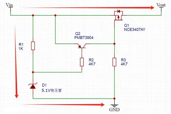
The voltage across resistor R1 is 0.7V (5.8V - 5.1V), resulting in a current of 0.7mA.
The base-emitter voltage of transistor Q2 is -0.6V (5.2V - 5.8V), causing Q2 to turn on.
With Q2 turned on, a current of 1.23mA flows through resistor R3 (5.8V / 4.7kΩ).
There are three current paths:
At this point, the gate-source voltage (Vgs) of MOSFET Q1 is 0, meaning Q1 does not conduct, indicating that the input voltage is too high. Consequently, the output voltage (Vout) is shut off, protecting the downstream load circuitry.
To modify the overvoltage protection circuit for a different voltage, simply replace the zener diode with one of a different zener voltage rating.


*To request free samples, please complete and submit the following information.
Our team will review your application within 24 hours and arrange shipment upon approval. Thank you!