Circuit Design Improvement Solution for Half-Bridge LLC No-Load Voltage Spike
In the half-bridge circuit, during no-load conditions, the duty cycle of the upper transistor is very small (possibly zero), resulting in a low voltage across the resonant capacitor at the bottom of the circuit. This can lead to the inability of the current flowing through the resonant inductor to reverse when the lower transistor conducts. Today, I'm sharing some valuable information I found online.
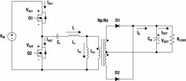
In the half-bridge circuit, when the lower transistor is turned off and the body diode of the lower transistor conducts for freewheeling, the upper transistor is turned on, causing an "instantaneous direct current." The direct current is forced to recover and turn off by the diode, resulting in a voltage drop across the parasitic inductance, which is superimposed on the lower transistor (in the off state).
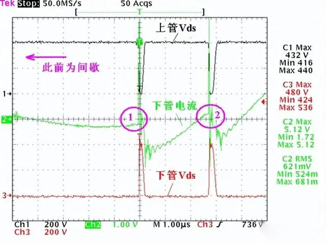
The main reason for the "instantaneous direct current" is the transient charging and discharging of the power transistor's gate-source capacitance and the reverse recovery of the diode.
To reduce the voltage spikes of the power transistor, power transistors with smaller gate-source capacitance and better recovery characteristics can be used. These transistors can quickly eliminate the direct current when the body diode is turned off, reducing voltage spikes.
Additionally, to reduce the conduction dead time of the upper and lower transistors, the upper transistor can be turned on when the lower transistor is turned off and the diode has not fully conducted. This reduces the reverse recovery current (the current passing through the power transistor's body and then turning off is smaller than the reverse recovery current when the current passes through the reverse diode and then turns off), thereby achieving the goal of reducing voltage spikes.
We conducted tests with dead times of 190nS and 120nS. Here are the results:
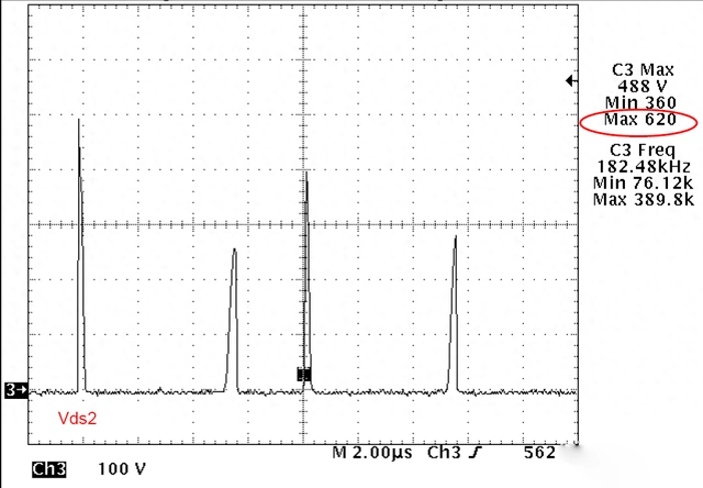
With a dead time of 190nS, the voltage spike of the lower transistor is 620V.
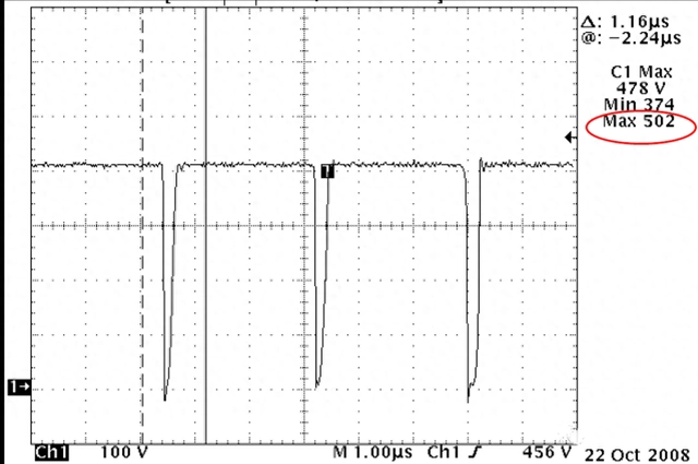
With a dead time of 120nS, the voltage spike of the lower transistor decreases to 496V, meeting the requirements for reduction.
It's important to note that if operating in the ZVS state, the dead time will not affect the voltage stress on the power transistor. However, if operating in a non-ZVS state, under no-load conditions, the voltage stress on both the power transistor and the output diode of the DC/DC converter is maximized. Therefore, if changes in the dead time lead to changes in the ZVS state of the power transistor, attention should also be paid to the voltage stress on the output diode of the DC/DC converter.



*To request free samples, please complete and submit the following information.
Our team will review your application within 24 hours and arrange shipment upon approval. Thank you!