What is Reverse Polarity Buck-Boost?
Reverse polarity Buck-Boost is a circuit topology that can generate negative voltage. It achieves voltage conversion from input to output by controlling the MOSFET switch through a power controller. When the MOSFET is closed, the inductor charges; when it is open, the inductor provides power to the output capacitor and load through the freewheeling diode, resulting in negative voltage output.
In basic circuit topologies, we have Buck, Boost, and Buck-Boost. Normally, the basic topology that can generate negative voltage is called Buck-Boost. Additionally, other circuits that achieve both step-up and step-down voltage conversion are also referred to as Buck-Boost. For clarity, the former is sometimes called reverse polarity Buck-Boost.
Regardless of whether it's stepping up or stepping down, basic topologies generally produce positive voltage. However, in Buck-Boost, negative voltage is produced.
For instance, if the input voltage is 12V and the output voltage is -5V, why is this the case?
In the reverse polarity Buck-Boost circuit, the power controller controls the gate voltage of the MOSFET to control its switching. The MOSFET is in a repeated switching process.
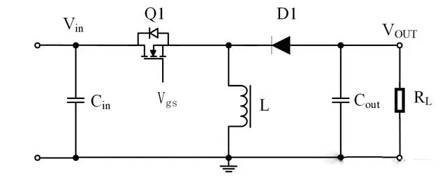
The buck-boost converter converts the positive DC voltage of the input voltage Vin into negative DC voltage Vout at the output.
When MOSFET Q1 is closed and conducts, the inductor L is connected across the power supply terminals, and the input voltage Vin charges the inductor. The current through the inductor gradually increases.
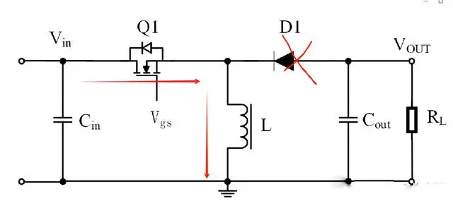
Since the current change rate (di/dt) is large during conduction transient, during this process, mainly Cin supplies power. At this time, Q1 acts as a short circuit, and the voltage across the ends of inductor L is Vin (input voltage). The output terminal Cout relies on its own discharge to provide energy to RL.
Since Q1 is conducting, the voltage across the ends of diode D1 is Vin and Vout, where Vout is negative, Vin is positive, and D1 is reverse-biased, equivalent to being turned off.
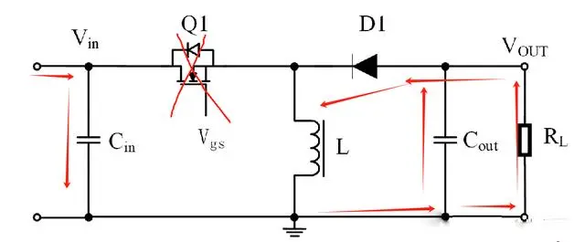
When Q1 is turned off, Vin charges the input capacitor. Since the current through the inductor cannot change suddenly, the inductor supplies power to the output capacitor Cout and the load RL through the freewheeling diode D1.
Since the direction of current through the inductor remains the same, the inductor charges the capacitor and also supplies power to the load RL.
The flow of current is: load resistance → Schottky diode → upper end of L1.
The lower end of RL is GND, meaning the voltage is 0V. The current direction through RL is from bottom to top. According to the current direction, the voltage at the upper end of RL (Vout) is lower than that at the lower end, resulting in a negative value.
Note:
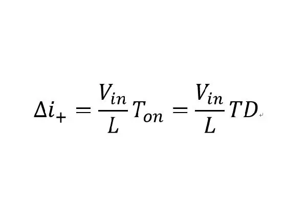
When the switch is on, the current on the inductor continuously increases to reach its maximum value (imax). The increase in current on the inductor during this time is due to the voltage acting on the inductor for energy storage, and this duration is the conduction time.
The formula is as follows:
Increment: Δi
Voltage: Vin



*To request free samples, please complete and submit the following information.
Our team will review your application within 24 hours and arrange shipment upon approval. Thank you!