The southern regions, being relatively humid, are less prone to static electricity generation, as shown in the reference figure below.

However, this doesn't mean MOSFETs are immune to static electricity! So, where does this static electricity come from?
Static Electricity Discharge:
It's a primary challenge in the manufacturing and use of most devices and ICs.
Electrostatic Discharge (ESD) is generally generated by humans and accumulates in the process of production, assembly, testing, storage, and transportation. While static electricity mainly arises from human body discharge (HBM), machine discharge (MM), component charging (CDM), and field induction (FIM), the former two are primarily tested modes.
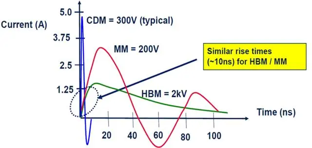
HBM: Industry standards for HBM ESD (MIL-STD-883C method 3015.7) specify an equivalent human body capacitance of 100pF and an equivalent human body resistance of 1.5Kohm.
MM: Static electricity generated by machine movement, when touching the chip, is discharged through the pin. The ESD standard for MM (EIA/JESD22-A115-A) specifies an equivalent machine resistance of 0 (metal, and the discharge time is short, between ms or us), with a capacitance of 100pF.
Due to the resistance being close to zero, the current is large. Additionally, the machine itself has many coupled wires, which can cause current interference and variations.
CDM: The device discharges after being charged with static electricity and comes into contact with a grounded conductor.
With the same static voltage level, the degree of damage to the device is: MM > CDM > HBM. Common specifications in product datasheets are HBM and MM, with the ESD standard for electronic devices being HBM contact 2KV.
After the above statements, do you understand why MOSFETs need to be protected from static electricity?
MOSFETs are sensitive to ESD as they have high input impedance and low gate-source capacitance, making them susceptible to external electromagnetic fields or static electricity induction.
MOSFET static breakdown occurs in two modes:
Voltage-type: Breakdown of the thin oxide layer on the gate forms pinholes, causing a short circuit between G-S or G-D.
Power-type: The metalized thin film aluminum strip is fused, resulting in an open circuit between G and S.
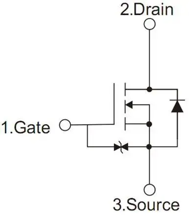
Most MOSFETs are rarely exposed to environments prone to ESD. However, in some applications, an ESD protection device is specifically added between GS to enhance its ESD protection capability.
However, nowadays, most MOSFETs are not so easily damaged, especially high-power VMOS, which generally have diode protection. Additionally, their gate capacitance is relatively large, making them less susceptible to induction of high voltage. Some CMOS devices internally add IO port protection, but CMOS device pins should not be touched directly with hands, as it may affect solderability.
Static Electricity Discharge:
Forms a short-lived large current, with the discharge pulse time constant generally much smaller than the device's heat dissipation time constant.
When the static discharge current flows through the pn junction, it generates a very high instantaneous power density, resulting in local overheating, even exceeding the material's own temperature (silicon's melting point is 1410℃), which will cause the pn junction to short circuit and the device to fail.
The smaller the power density, the less susceptible the device is to damage.
Relative to other devices, MOSFETs are slightly more sensitive to ESD. However, ESD is random, so even if ESD occurs, it may not necessarily cause the MOSFET to breakdown.
Solutions:
During storage and transportation, it is best to use metal containers or packaging materials, and avoid synthetic fiber products.
During assembly and debugging, tools, instruments, and workbenches should be properly grounded, and operators should avoid wearing nylon or synthetic clothing to prevent static interference.
MOSFETs are voltage-driven devices, and the floating gate is susceptible to external interference, causing the MOS to conduct, and external interference signals charge the GS junction capacitor. Floating G is dangerous, as it can cause the MOS to burst. Connecting a pull-down resistor to ground for the G pin prevents external interference signals from passing directly. Generally, this gate resistor can be 10-20K.
The role of this gate resistor was mentioned before:
Provide bias voltage to the MOS
Act as a leakage resistor
That's all for this issue, thank you for watching~
VBsemi


*To request free samples, please complete and submit the following information.
Our team will review your application within 24 hours and arrange shipment upon approval. Thank you!