Explanation of MOSFET Soft Start Circuit with Example
Why do we need power-on start? What can power-on soft start do?
Soft start, as the name suggests, is to slowly turn on the circuit power supply.
Explanation seems simple, but is the working principle the same?
Today, we discuss the application analysis of power-on soft start with the above questions in mind.
Firstly, why do we need power-on soft start?
Let's take the common function "hot plug" in electronic systems as an example.
(Hot plug: In normal operation of the system, plug and unplug a unit of the system under power without affecting the system.)
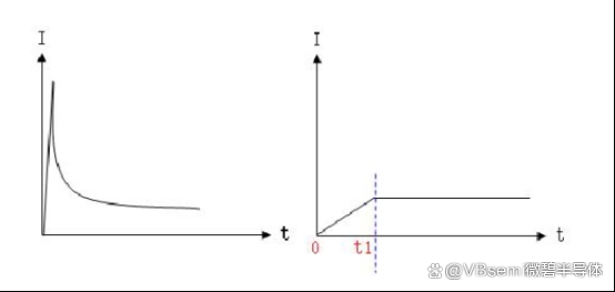
Hot plugging generally has two effects on electronic systems: 1. During hot plugging, the mechanical contacts of the connector will bounce at the moment of contact, causing power supply oscillation; 2. During hot plugging, due to the charging effect of the system's large-capacity storage capacitors, a large surge current will occur in the system.
Due to the above reasons, especially the instantaneous large current, obvious sparking will occur during operation, which can cause electromagnetic interference and corrosion to the connectors. Therefore, a "slow" power-on is needed.
Here, we can deduce the two main functions of the soft start circuit: 1. Anti-jitter delay power-on 2. Control the rise slope and amplitude of the input current.
Next, we will use a MOSFET to explain the working principle of a soft start circuit.
MOSFET has the advantages of low on-state resistance (Rds_on) and simple drive, which, combined with other components, can form a slow start circuit.
Usually, a PMOS is used in the positive power supply and an NMOS is used in the negative power supply.
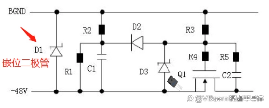
As shown below: a -48V power supply soft start circuit diagram built with a VBsemi NMOS.
First, let's briefly explain the "other components":
D1 (TVS diode): Generally used for surge protection in power circuits to prevent damage to the subsequent circuit due to excessive input voltage before the MOSFET conducts;
D2 (Schottky diode): Isolation of anti-jitter delay circuit and power-on slope control circuit (to prevent interference from C1);
D3 (Zener diode): Ensure the stability of VGS voltage and protect the gate-source of MOSFET Q1 from high voltage breakdown;
R2/R1 and C1: R1 provides a fast discharge path for C1; The voltage division value of R1/R2 is greater than the stabilizing voltage of D3;
R3 and C2: Control the rise slope of the power supply voltage;
R4 and R5: Prevent MOSFET self-excitation oscillation.
In the diagram above, Q1 is the MOSFET, Cgs is the parasitic capacitance between its gate and source, Cgd is the parasitic capacitance between gate and drain, and Cds is the parasitic capacitance between drain and source.
It can be seen that an external capacitor C2 is connected in parallel with the gate and drain, and the total capacitance of the gate and drain, C'gd = C2 + Cgd, is almost equal to C2 relative to C2.
The gate turn-on voltage Vth of the MOSFET is Vw under normal operation, where the voltage is equal to the embedded voltage of the stabilizing diode D3. The charging time constant of C1 is t = (R1//R2//R3)C1, and since R3 is usually much larger than R1 and R2, t ≈ (R1//R2)C1.
The working process of this circuit can be divided into four stages:
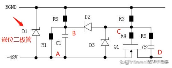
As shown in the figure: A, B are anti-jitter circuits; C, D are voltage soft start circuits.
First stage:
The -48V power supply charges C1, and after Q1 is turned on, the drain current starts to increase. At this time, the rate of change is proportional to the transconductance of the MOSFET and the rate of change of the gate-source voltage; at this time:
The voltage VA decreases rapidly with the input; The voltage VB drops to -48V momentarily, then slowly rises to charge C1 at both ends; The voltage VC is pulled down by Vb and D2 conducts slightly higher than VB. With the charging of R1/R2 to C1, the VGS (=Vc-Va) also increases, and Q1 is in the cutoff state.
When Q1 is in the cutoff state, i.e., Vd=0V, since C2 is charged instantaneously through R5, the Vcd voltage and the initial voltage of C2 are both -47.6V, and then slowly discharge as the voltage VC rises.
R3 flows through D2 to R1, the VB point voltage starts to rise slowly from -48V, and the Vc voltage rises slowly from -47.6V;
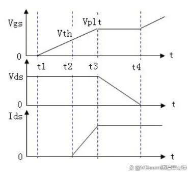
(Change of Vgs, Vds, and Ids at startup)
Second stage:
The VGS voltage VGS(th) rises to Vplt, and MOSFET Q1 is fully open.
Generally, it is best to end the anti-jitter circuit action before the Miller platform, and the startup time thereafter is controlled by the voltage soft start circuit; it depends on the time for R1/R2 to charge C1 to VGS(th), including the calculation of the charging time of R3 and C2.
Third stage:
At this point, the Miller platform stage is reached. As the drain current (Idrain) continues to increase, the load terminal voltage VD starts to decrease from 0V, and the Miller platform stage begins;
Generally, the maximum input current of the device is at the moment of startup, before the device power supply voltage starts to rise, at which time Q1 can limit the size of the surge current through its own voltage drop;
The Id current is maintained at ID, and the Vds voltage decreases.
Fourth stage:
After the Miller platform stage ends, Vd remains at -48V; Id current is still maintained at ID, and Vds voltage decreases to a lower value, but the slope and amplitude of the decrease are small, and finally stabilizes.
Usually, after the Miller platform ends, the MOSFET is basically turned on.
Application of VBsemi MOSFET
From the above, we can see that the MOSFET is a very important device in the field of switching power supplies.
VBsemi's MOSFET is very suitable for low-voltage, high-current, medium-power applications, etc., due to its fast switching speed and strong current-carrying capacity, effectively improving the power conversion efficiency. Its importance is as follows, but not limited to:
The switch (upper tube) and freewheeling diode (lower tube) of the switching power supply can be realized through the MOSFET, and the on/off time of the upper and lower tubes determines the switch loss of the MOSFET:
During the conduction process, from the MOSFET opening to the end of the Miller platform, is a key stage of the switch conduction.
Above is what we talked about today, follow us for more exciting content next time!

*To request free samples, please complete and submit the following information.
Our team will review your application within 24 hours and arrange shipment upon approval. Thank you!